- Remaining Timing :-
(1). When p-n junction diode is forward biased then
- (a). both the depletion region and barrier height are reduced
- (b). the depletion region is widened and barrier height is reduced
- (c). the depletion region is reduced and barrier height is increased
- (d). both the depletion region and barrier height are increased
- (e). None of these
Explanation:
(2). The electrical conductivity of a semiconductor increases when electromagnetic radiation of wavelength shorter than 2480nm is incident on it. the band gap in (eV) for the semiconductor is
- (a). 2.5eV
- (b). 1.1eV
- (c). 0.7eV
- (d). 0.5eV
- (e). None of these
Explanation:
(3). Carbon silicon and germanium have four valence electrons each. At room temperature which one of the following statements is most appropriate?
- (a). the number of free electrons for conduction is significant only in si and ge but small in C
- (b). the number of free conduction electrons is significant in C but small in si and ge
- (c). the number of free conduction electrons is negligibly small in all the three
- (d). the number of free electrons for conduction is significant in all the three
- (e). None of these
Explanation:
(4). A working transistor with its three legs marked P,Q and R is tested using a multimeter. No conduction is found between P and Q. by connecting the common(negative) terminal of the multimeter to R and the other (positive) terminal to P or Q, some resistance is seen on the multimeter. which of the following is true for the transistor?
- (a). it is an npn transistor with R as base
- (b). it is a pnp transistor with R as collector
- (c). it is a pnp transistor with R as emitter
- (d). it is an npn transistor with R as collector
- (e). None of these
Explanation:

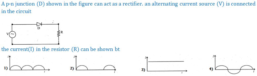
- (a). 1
- (b). 2
- (c). 3
- (d). 4
- (e). None of these
Explanation:

- (a). 49
- (b). 50
- (c). 54
- (d). 48
- (e). None of these
Explanation:
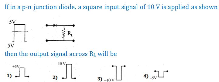
- (a). 1
- (b). 2
- (c). 3
- (d). 4
- (e). None of these
Explanation:
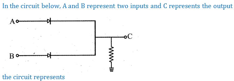
- (a). NOR gate
- (b). AND gate
- (c). NAND gate
- (d). OR gate
- (e). None of these
Explanation:
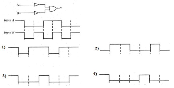
- (a). 1
- (b). 2
- (c). 3
- (d). 4
- (e). None of these
Explanation:
- (a). 1
- (b). 2
- (c). 3
- (d). 4
- (e). None of these
Explanation:
Recent Updates
ACHIEVER GALLERY


Word of Mouth