
- Remaining Timing :-
(1). If a small amount of antimony is added tp germanium crystal
- (a). it becomes a p-type semiconductor
- (b). the antimony becomes an acceptor atom
- (c). there will be more free electrons than holes in the semiconductor
- (d). its resistance is increased
- (e). None of these
Answer : there will be more free electrons than holes in the semiconductor
Explanation:
(2). In a n-type semiconductor which of the following statement is true?
- (a). electrons are minority carriers and pentavalent atoms are dopants
- (b). holes are minority carriers and pentavalent atoms are dopants
- (c). holes are majority carries and trivalent atoms are dopants
- (d). electrons are majority carries and trivalent atoms are dopants
- (e). None of these
Answer : holes are minority carriers and pentavalent atoms are dopants
Explanation:
(3). 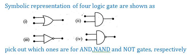
- (a). II,III and IV
- (b). III,II and I
- (c). III,III and IV
- (d). II,IV and III
- (e). None of these
Answer : II,IV and III
Explanation:
(4). 
- (a). 1
- (b). 2
- (c). 3
- (d). 4
- (e). None of these
Answer : 4
Explanation:
(5). A zener diode, having breakdown voltage equal to 15C, is used in a voltage regulator circuit shown in figure. the current through the diode is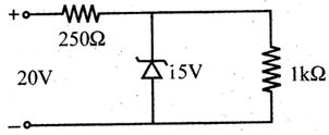
- (a). 10mA
- (b). 15mA
- (c). 20mA
- (d). 5mA
- (e). None of these
Answer : 5mA
Explanation:
(6). Two ideal diodes are connected to a battery as shown in the circuit. the current supplied by the battery is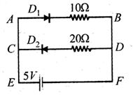
- (a). 0.75 A
- (b). zero
- (c). 0.25A
- (d). 0.5A
- (e). None of these
Answer : 0.5A
Explanation:
(7). 
- (a). 0.1V
- (b). 1.0V
- (c). 1mV
- (d). 10mV
- (e). None of these
Answer : 10mV
Explanation:
(8). 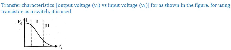
- (a). in region(III)
- (b). both in region I and III
- (c). in region II
- (d). in region I
- (e). None of these
Answer : both in region I and III
Explanation:
(9). The figure shows a logic circuit with two inputs A and B and the output C. the voltage wave forms across A,B and C are as given, the logic gate circuit is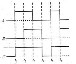
- (a). OR gate
- (b). NOR gate
- (c). AND gate
- (d). NAND gate
- (e). 1 and 2
Answer : 1 and 2
Explanation:
(10). 
- (a). 2000
- (b). 3000
- (c). 4000
- (d). 1000
- (e). None of these
Answer : 2000
Explanation:
Recent Updates
ACHIEVER GALLERY

Result On Nov-2016

Result On Nov-2016

Result On Nov-2016
Word of Mouth
Feedback about SALEM

Feedback about ERODE

Feedback about DHARMAPURI