
- Remaining Timing :-
(1). In a p-n junction photo cell, the value of the photo-electromotive force produced by monochromatic light is proportional to
- (a). the voltage applied at the p-n junction
- (b). the barrier voltage at the p-n junction
- (c). the intensity of the light falling on the cell
- (d). the frequency of the light falling on the cell
- (e). None of these
Explanation:
(2). choose the only false statement from the following
- (a). in conductors the valence and conduction bands may overlap
- (b). substances with energy gap of the order of 10 e V are insulators
- (c). the resistivity of a semiconductor increases with increase in temperature
- (d). the conductivity of a semiconductor increases with increase in temperature
- (e). None of these
Explanation:
(3). Which one of the following statement is false?
- (a). pure si doped with trivalent impurities gives a p-type semiconductor
- (b). majority carriers in a n-type semiconductor are holes
- (c). minority carriers in a p-type semiconductor are electrons
- (d). the resistance of intrinsic semiconductor decreases with increase of temperature
- (e). None of these
Explanation:
(4). The device that can act as a complete electronic circuit is
- (a). junction diode
- (b). integrated circuit
- (c). junction transistor
- (d). zener diode
- (e). None of these
Explanation:
(5). A common emitter amplifier has a voltage gain of 50, an input impedance of 100? and an output impedance of 200? the power gain of the amplifier is
- (a). 500
- (b). 1000
- (c). 1250
- (d). 50
- (e). None of these
Explanation:
(6). For transistor action A) base, emitter and collector regions should have similar size and doping concentrations B) the base region must be very thin and lightly doped C) the emitter-base junction is forward biased and base-collector junction is reverse based D) both the emitter-base junction as well as the base-collector junction are forward biased
- (a). C and D
- (b). D and A
- (c). A and 2
- (d). B and C
- (e). None of these
Explanation:
(7). In following biasing of the p-n junction
- (a). the positive terminal of the battery is connected to p-side and the depletion region becomes thick
- (b). the positive terminal of the battery is connected to n-side and the depletion region becomes thin
- (c). the positive terminal of the battery is connected to n-side and the depletion region becomes thick
- (d). the positive terminal of the battery is connected to p-side and the depletion region becomes thin
- (e). None of these
Explanation:
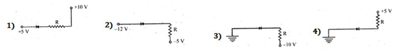
- (a). 1
- (b). 2
- (c). 3
- (d). 4
- (e). None of these
Explanation:
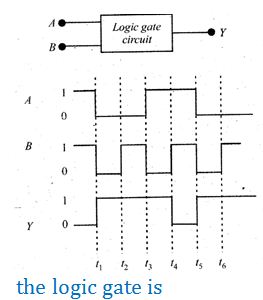
- (a). NAND gate
- (b). NOR gate
- (c). OR gate
- (d). AND gate
- (e). None of these
Explanation:

- (a). 50
- (b). 75
- (c). 100
- (d). 25
- (e). None of these
Explanation:
Recent Updates
ACHIEVER GALLERY


Word of Mouth