
- Remaining Timing :-
(1). In a P-N junction
- (a). the potential of P&N sides becomes higher alternately
- (b). the P side is at higher electrical potential than N side
- (c). the N side is at higher electric potential than P side
- (d). both P&N sides are at same potential
- (e). None of these
Answer : the P side is at higher electrical potential than N side
Explanation:
(2). Barrier potential of a P-N junction diode does not depend on
- (a). doping density
- (b). diode design
- (c). temperature
- (d). forward bias
- (e). None of these
Answer : diode design
Explanation:
(3). A n-p-n transistor conducts when
- (a). both collector and emitter are negative with respect to the base
- (b). both collector and emitter are positive with respect to the base
- (c). collector is positive and emitter is negative with respect to the base
- (d). collector is positive and emitter is at same potential as the base
- (e). None of these
Answer : collector is positive and emitter is negative with respect to the base
Explanation:
(4). Reverse bias applied to a junction diode
- (a). increases the minority carrier current
- (b). lowers the potential barrier
- (c). raises the potential barrier
- (d). increases the majority carrier current
- (e). None of these
Answer : raises the potential barrier
Explanation:
(5). In semiconductors at a room temperature
- (a). the conduction band is completely empty
- (b). the valence band is partially empty and the conduction band is partially filled
- (c). the valence band is completely filled and the conduction band is partially filled
- (d). the valence band is completely filled
- (e). None of these
Answer : the valence band is completely filled and the conduction band is partially filled
Explanation:
(6). The forward biased diode is
- (a). 1
- (b). 2
- (c). 3
- (d). 4
- (e). None of these
Answer : 4
Explanation:
(7). A d.c. battery of V volt is connected to a series combination of a resistor R and an ideal diode D as shown in the figure below. the potential difference across R will be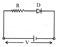
- (a). 2v when diode is forward biased
- (b). zero when diode is forward biased
- (c). V when diode is reverse biased
- (d). V when diode is forward biased
- (e). None of these
Answer : V when diode is forward biased
Explanation:
(8). 
- (a). 6
- (b). 48
- (c). 24
- (d). 12
- (e). None of these
Answer : 24
Explanation:
(9). Following diagram performs the logic function of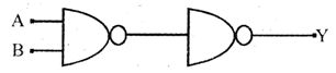
- (a). XOR gate
- (b). AND gate
- (c). NAND gate
- (d). OR gate
- (e). None of these
Answer : AND gate
Explanation:
(10). The peak voltage in the output of a half-wave diode rectifier fed with a sinusoidal signal without filter is 10v. the d.c. component of the output voltage is
- (a). 1
- (b). 2
- (c). 3
- (d). 4
- (e). None of these
Answer : 3
Explanation:
Recent Updates
ACHIEVER GALLERY

Result On Nov-2016

Result On Nov-2016

Result On Nov-2016
Word of Mouth

Feedback about SALEM

Feedback about ERODE

Feedback about DHARMAPURI